


AF90Degree10.0Copper shell rear two pins without curled edge reverse heightened type8.70HWhite gluePBT Not High Temperature Resistant
- Manufacturer
- MFR.Part #
- AF90Degree10.0Copper shell rear two pins without curled edge reverse heightened type8.70HWhite gluePBT Not High Temperature Resistant
- JLCPCB Part #
- C168712
- Package
- Plugin
- Description
- 1 4P Female Type-A USB 2.0 插件 USB Connectors ROHS
- EasyEDA Libraries
- Datasheet
- Source
- JLCPCB
- Assembly Type
- Wave Soldering
- PCBA Type
- Economic and Standard
Note: The purchased components are stored in your JLCPCB parts library for future PCBA orders only, and cannot be shipped separately.
| Attributes | Value | |
|---|---|---|
| Category | Connectors/USB Connectors | |
| Manufacturer | Jing Extension of the Electronic Co. | |
| Package | Plugin | |
| Number of Ports | 1 | |
| Connector Type | Type-A | |
| Number of Contacts | 4P | |
| Gender | Female | |
| Protocol Standard | USB 2.0 |
* Images are for reference only
AF90Degree10.0Copper shell rear two pins without curled edge reverse heightened type8.70HWhite gluePBT Not High Temperature Resistant
Extended- Manufacturer
- MFR.Part #
- AF90Degree10.0Copper shell rear two pins without curled edge reverse heightened type8.70HWhite gluePBT Not High Temperature Resistant
- JLCPCB Part #
- C168712
- Package
- Plugin
- Description
- 1 4P Female Type-A USB 2.0 插件 USB Connectors ROHS
- EasyEDA Libraries
- Datasheet
- Source
- JLCPCB
- Assembly Type
- Wave Soldering
- PCBA Type
- Economic and Standard
Note: The purchased components are stored in your JLCPCB parts library for future PCBA orders only, and cannot be shipped separately.
* Images are for reference only
AF90Degree10.0Copper shell rear two pins without curled edge reverse heightened type8.70HWhite gluePBT Not High Temperature Resistant
Extended- Manufacturer
- MFR.Part #
- AF90Degree10.0Copper shell rear two pins without curled edge reverse heightened type8.70HWhite gluePBT Not High Temperature Resistant
- JLCPCB Part #
- C168712
- Package
- Plugin
- Description
- 1 4P Female Type-A USB 2.0 插件 USB Connectors ROHS
- EasyEDA Libraries
- Datasheet
- Source
- JLCPCB
- Assembly Type
- Wave Soldering
- PCBA Type
- Economic and Standard
Note: The purchased components are stored in your JLCPCB parts library for future PCBA orders only, and cannot be shipped separately.
AF90Degree10.0Copper shell rear two pins without curled edge reverse heightened type8.70HWhite gluePBT Not High Temperature Resistant Specifications
AF90Degree10.0Copper shell rear two pins without curled edge reverse heightened type8.70HWhite gluePBT Not High Temperature Resistant technical specifications, attributes, and parameters.
| Attributes | Value | |
|---|---|---|
| Category | Connectors/USB Connectors | |
| Manufacturer | Jing Extension of the Electronic Co. | |
| Package | Plugin | |
| Number of Ports | 1 | |
| Connector Type | Type-A | |
| Number of Contacts | 4P | |
| Gender | Female | |
| Protocol Standard | USB 2.0 |
PCB Assembly Tips
From components to fully assembled PCBs. JLCPCB supports PCB assembly for the AF90Degree10.0Copper shell rear two pins without curled edge reverse heightened type8.70HWhite gluePBT Not High Temperature Resistant. Sign up to receive and start your assembly today →
- 1
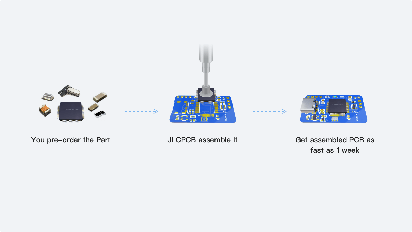
Step 1 - Pre-order the parts you need from JLCPCB.
- 2
Step 2 - Place a PCBA order to have those parts assembled onto your boards.
- 3
Step 3 - JLCPCB manufactures and assembles your boards in as fast as 3 days.
AF90Degree10.0Copper shell rear two pins without curled edge reverse heightened type8.70HWhite gluePBT Not High Temperature Resistant Documents
AF90Degree10.0Copper shell rear two pins without curled edge reverse heightened type8.70HWhite gluePBT Not High Temperature Resistant datasheets or manufacturer documentation.
AF90Degree10.0Copper shell rear two pins without curled edge reverse heightened type8.70HWhite gluePBT Not High Temperature Resistant Schematic Symbol & PCB Footprint
The AF90Degree10.0Copper shell rear two pins without curled edge reverse heightened type8.70HWhite gluePBT Not High Temperature Resistant schematic symbol and PCB footprint are available in the EasyEDA PCB design tool.