
Note: The purchased components are stored in your JLCPCB parts library for future PCBA orders only, and cannot be shipped separately.
| Attributes | Value | |
|---|---|---|
| Category | Switches/Multi-Directional Switches | |
| Manufacturer | C&K | |
| Package | - |
* Images are for reference only
QSA4S 3.5N H1 G8
Extended- Manufacturer
- MFR.Part #
- QSA4S 3.5N H1 G8
- JLCPCB Part #
- C19417660
- Package
- -
- Description
- - Multi-Directional Switches ROHS
- EasyEDA Libraries
- ECCN
- -
- Datasheet
- Source
- JLCPCB
- Assembly Type
- Wave Soldering
- PCBA Type
- Economic and Standard
- MSL Level
- MSL 1
Note: The purchased components are stored in your JLCPCB parts library for future PCBA orders only, and cannot be shipped separately.
* Images are for reference only
- Manufacturer
- MFR.Part #
- QSA4S 3.5N H1 G8
- JLCPCB Part #
- C19417660
- Package
- -
- Description
- - Multi-Directional Switches ROHS
- EasyEDA Libraries
- ECCN
- -
- Datasheet
- Source
- JLCPCB
- Assembly Type
- Wave Soldering
- PCBA Type
- Economic and Standard
- MSL Level
- MSL 1
Note: The purchased components are stored in your JLCPCB parts library for future PCBA orders only, and cannot be shipped separately.
QSA4S 3.5N H1 G8 Specifications
QSA4S 3.5N H1 G8 technical specifications, attributes, and parameters.
| Attributes | Value | |
|---|---|---|
| Category | Switches/Multi-Directional Switches | |
| Manufacturer | C&K | |
| Package | - |
PCB Assembly Tips
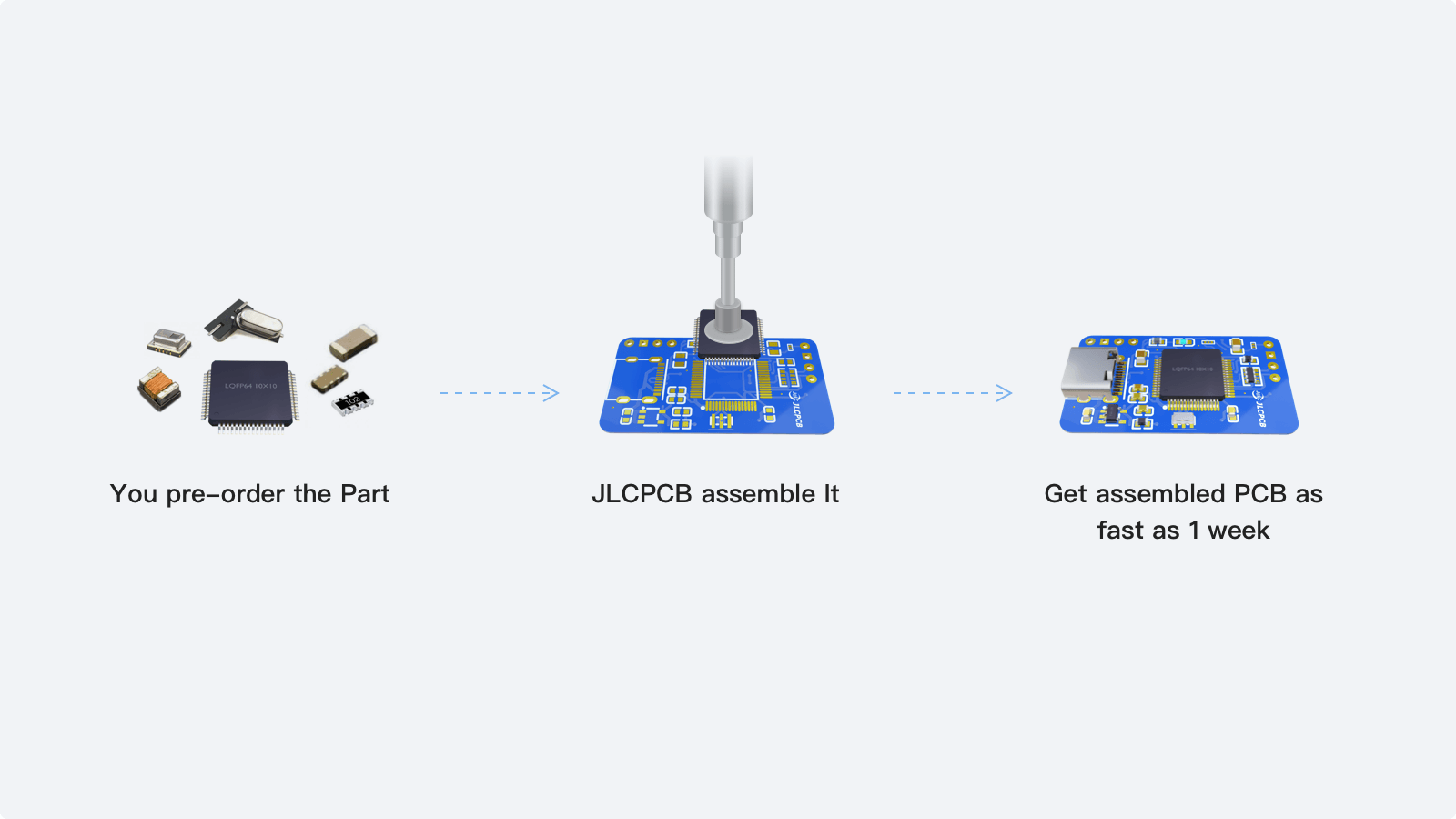
From components to fully assembled PCBs. JLCPCB supports PCB assembly for the QSA4S 3.5N H1 G8. Sign up to receive and start your assembly today →
- 1
Step 1 - Pre-order the parts you need from JLCPCB.
- 2
Step 2 - Place a PCBA order to have those parts assembled onto your boards.
- 3
Step 3 - JLCPCB manufactures and assembles your boards in as fast as 3 days.
QSA4S 3.5N H1 G8 Documents
QSA4S 3.5N H1 G8 datasheets or manufacturer documentation.
Datasheet: QSA4S 3.5N H1 G8 Datasheet (PDF)
QSA4S 3.5N H1 G8 Schematic Symbol & PCB Footprint
The QSA4S 3.5N H1 G8 schematic symbol and PCB footprint are available in the EasyEDA PCB design tool.