JLCPCB's 6-20 Layers PCBs: Free Upgrade to ENIG 2u"
JLCPCB's 6-20 Layers PCBs: Free Upgrade to ENIG 2u"
JLCPCB has been dedicated to providing advanced multi-layer PCBs, ranging from 6 to 20 layers, that have received immense praise and recognition from countless customers. To fulfill our commitment to accelerating global hardware innovation and enabling more users to economically and efficiently complete their projects, we introduced free PCB assembly services last year.
Furthermore, we are delighted to announce the introduction of our Free Upgrade Immersion Gold Thickness service. This enhancement aims to elevate the quality of PCBs without incurring any additional costs. We take pride in continuously improving our offerings, ensuring that our customers benefit from the highest-quality PCBs while maintaining affordability.
For all 6-20 layer PCBs, we are upgrading the immersion gold thickness to 2u" at no additional cost!
The Introduction of JLCPCB Free Upgrade to ENIG 2u" Service
Compared to 1u", 2u" gold thickness provides double the thickness, resulting in higher production costs. Many manufacturers in the industry usually impose an additional fee for this increased thickness. However, JLCPCB is pleased to inform you that we will not impose any extra fees. This means you can enjoy the benefits of the enhanced quality without any additional cost.
If you choose a board thickness of 6 layers or more, there is no need to make any selections as the default choice for gold thickness will be 2u".
The upgraded order interface is as follows:
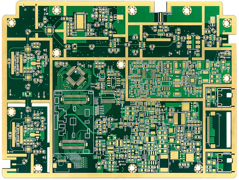
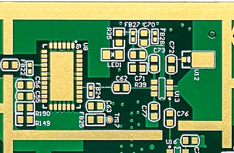
The Showcase of JLCPCB ENIG Surface Finished PCBs
Here are the samples of JLCPCB ENIG surface finished PCBs:
Zoomed-in Effect:
The introduction of JLCPCB Via-in-Pad Technology
Currently, JLCPCB is offering free POFV (Plated Over Filled Via) via-in-pad technology for 6-20 layer PCBs, while other companies typically charge expensive fees for this feature.
Via-in-pad, as the name suggests, involves drilling holes within the solder pads. JLCPCB’s improved process is called POFV. It allows flexible, compact routing and makes connections more robust and reliable than with regular vias. This technology is commonly used in high-end products but has been limited in terms of affordability and widespread adoption due to its high cost. However, PCBs designed with via-in-pad technology surpass traditional methods such as solder mask covering or filling. They not only exhibit superior aesthetics but also deliver enhanced performance. Additionally, the adoption of via-in-pad design significantly reduces design time and improves product quality.
The Showcase of JLCPCB via-in-pad PCBs
Here are the samples of PCBs produced using JLCPCB via-in-pad technology:
Zoomed-in Effect:
Experience the Next Level of PCB Manufacturing with JLCPCB! Upgrade your PCB order today and elevate your projects to new heights with JLCPCB's "2u" gold thickness + POFV via-in-pad technology.
Related Articles:
- What is PCB Via and Which Type Should You Choose?
- The True Cost of Custom PCBs
- Comparison of BGA vs LGA in High-Power Applications
- Everything You Need to Know about BGA Technology in PCB Assembly
- Enhanced PCB Design Efficiency with Mouse Bites
- A Comprehensive Guide on How to Read and Interpret Resistor Color Codes
Recent Posts
• JLCPCB $4.5/㎡ Off on Quality 4-Layer PCBs
Apr 25, 2024
• Flex PCB Now Available at JLCPCB From Special Offer of $15
Apr 25, 2024
• JLCPCB's Free Via-in-Pad Process Boosts PCB Design Efficiency by 200%
Apr 17, 2024
• From Concept to Production: JLCPCB Launches Full-Service PCB Design Solution
Apr 12, 2024
• Breaking Stereotypes with JLCPCB's New Service: Multi-color Silkscreen PCB
Apr 1, 2024