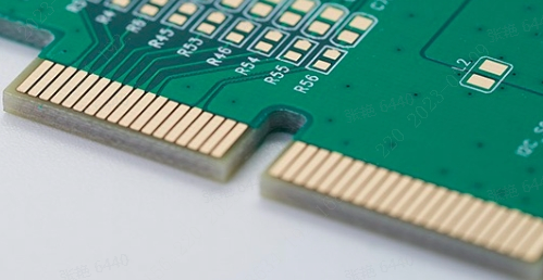
Gold fingers are the gold-plated columns along the connecting edges of printed circuit boards (PCBs), please see the following picture for reference. Gold fingers are served as the connecting contacts between motherboards and components like graphics or sound cards. PCB gold fingers are also used in various other devices that communicate via digital signals, such as smartphones and smartwatches. Gold is used for the connecting point along a PCB because of the alloy's superior conductivity.
1. Basically, only when ENIG is chosen, the fingers for your PCB will be with gold, if you choose HASL surface treatment, then it will be covered with tin.
2. Chamfers are not available on boards smaller than 5x5cm.
3. If there is fingers in your file and it is panel with v-cut, then the fingers can not be made with chamfer since the fingers will be in the middle of the PCB.
4. Please kindly ensure the design matches the rule below to avoid the fingers being too short or the remaining thickness of the board being too thin after the bevel, making the gold fingers unusable.
PCB Thickness | Regular Bevel Height | CAM Copper Cutting | The Production Bevel Height (when the gold finger is far from the forming edge) |
0.4-1.6mm | 0.50mm | 0.60mm on one side | 0.90±0.10mm on one side |
2.0mm | 0.65mm | 0.75mm on one side | 1.05±0.10mm on one side |
Note: The production of the bevel is subject to not hurting the gold fingers.
Chamfer depth
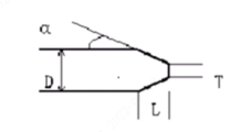
Chamfer depth calculation formula: L= (D/2 - T/2) /t gα
D: PCB Thickness (mm) T: Remaining Thickness of Board (mm)
α: Chamfer Angle L: Chamfer Depth(mm)
(Length of the beveling cut from finger to the board edge)
By default, the chamfer Angle is 30°, and the remaining thickness of the board is 0.5mm. To ensure the bevel does not hurt the gold finger, the chamfer depth of 1.6mm thickness board shall be 0.6mm(the distance L from the edge of the board to the gold finger shall be at least 0.6mm). Please kindly refer to this rule when designing. Otherwise, part of the gold finger will be cut off.
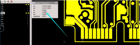
Example:
The green part is the original Gerber file, while the yellow part is the optimized production file.
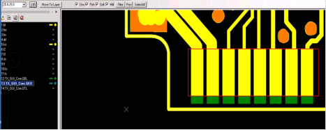
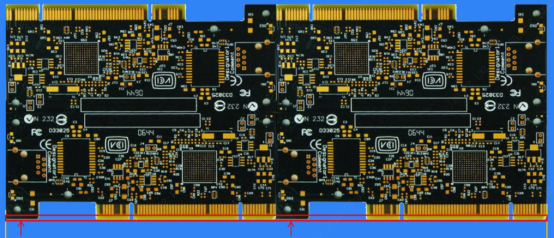
The red frame indicates the beveled area. When designing, please kindly pay attention that this area can not have copper. Otherwise, after the bevel, the trace will be damaged and the copper will be exposed.
The length and width of a single board or panel with gold fingers shall not be less than 50mm.
 Live Chat


 My Coupons
 Sign out


